FlatCAM practical tutorial: silkscreen geometry – Part 4
Another essential feature is milling inside objects to create elements or write letters over PBC.
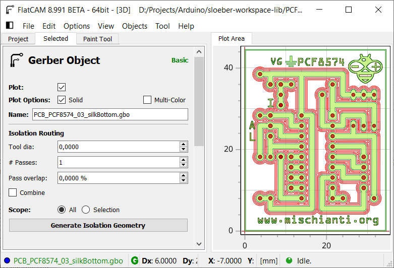
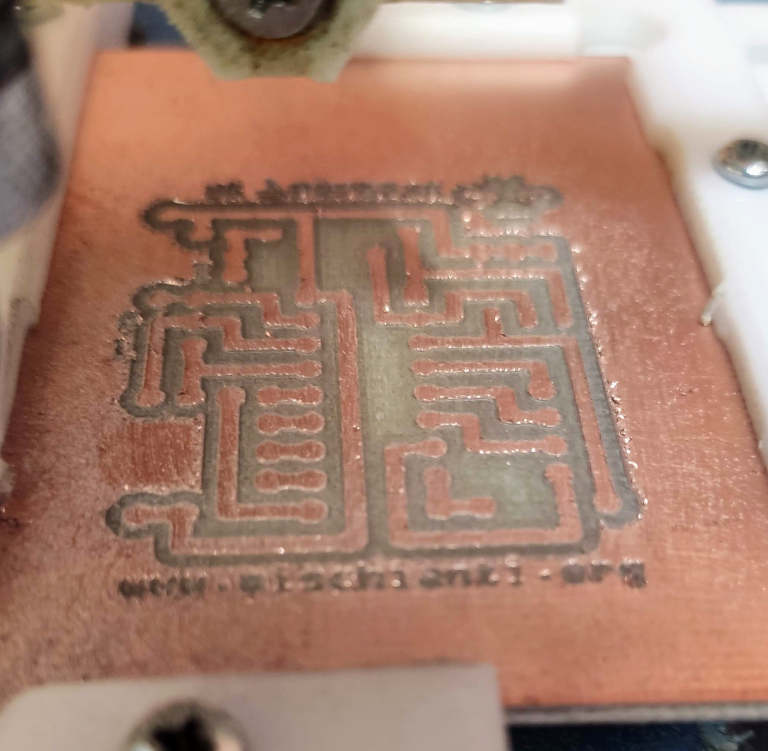
I load the schema of my test PCB again.
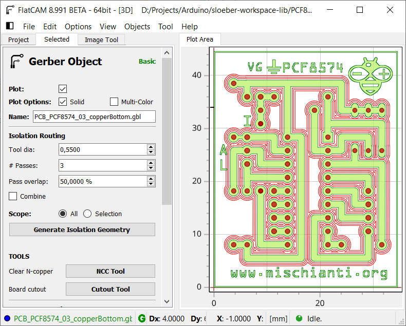
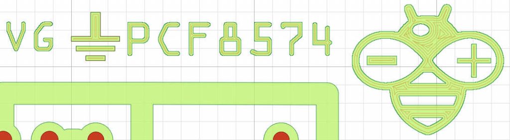
As you can see in the image, I add some letters and my logo; the better way to write them is to use paint features.
First, you must generate a geometry over Gerber to create a delimiter contour for generating internal geometry.
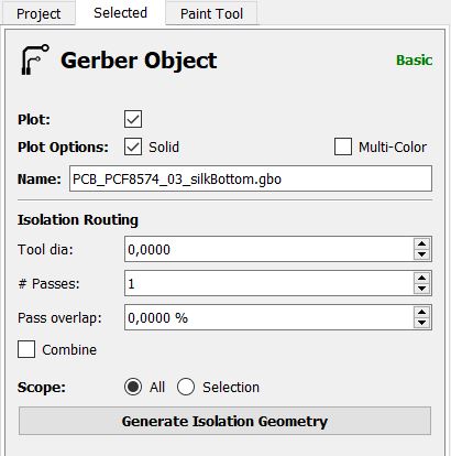
You can set the parameters Tool dia and Pass overlap to 0, the result is this
ok, it seems nothing changes, but if you pay more attention, the green of silkscreen Gerber is darker now because you have created a geometry over a Gerber, and It’s difficult to see; you can add a little margin to manage a letter less thin.
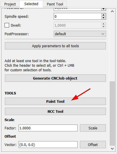
Paint tool
We have a container to generate a paint, so select the geometry created.
Paint tools have a lot of parameters, and you must learn the better for every need. It’s very similar to Non-Copper cleaning but with some selectable options.
As Non-Copper cleaning, you can select multi-tools and various methods, but for our scope, we don’t use anything of that, we want only write some letter and a little logo, other options are more suitable for biggest silkscreen.
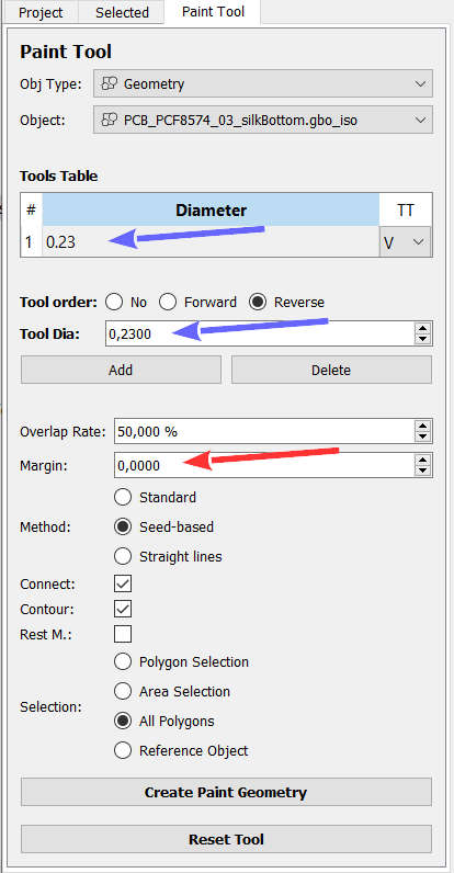
As you can see, I insert a minimal diameter because our scope is to write some letters too little for our Tool, but It’s sufficient that it is readable. This little value cannot be adequate for the smallest letters because if letters are too thin, nothing is painted; for example, now I’m going to apply the parameter you read upper to all geometry of silkBottom file, so I select All Polygons and click Create Paint Geometry.
Now you can see that some letter is perfectly managed
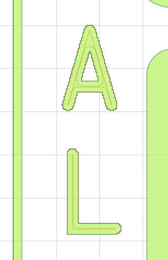
and here some letter thinner have problem with this Tool Dia too big
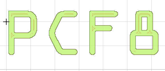
So the solution is simple, you must generate a paint geometry fitted for every set of letters, you must reduce the Tool Dia to fit perfectly every letter.
You can use two selection types.
- Polygon selection: every time you click on Create Paint Geometry you are going to select a letter or othe geometry (of reference object selected on the upper of panel);
- Area selection: you can select a set of elements (letters or other) using the selection tool, when you click on the button the selection starts from the corner and the next click closes the selection and when you click with the right mouse button the action is performed for the whole area you have created.
You can use paint to write or create a tiny logo with your CNC
Method explained
I usually select a standard method to fill elements with geometry, I think this solution is pretty good, but we can choose other systems; here are the three different ways:
Standard method
For me, the best, simple, and most powerful
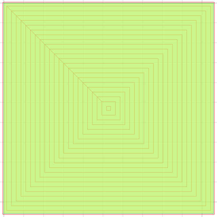
It starts from the outer perimeter and follows the shape until it covers the entire surface.
Seed-based method
As you can understand from the name, you will plant a seed, growing circularly.
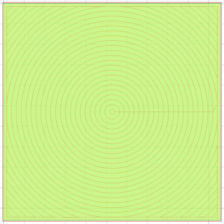
Not so good in many circumstances; you risk having a lot of lift for no reason.
Straight line method
Simply It starts to mill a series of horizontal lines from top to bottom.
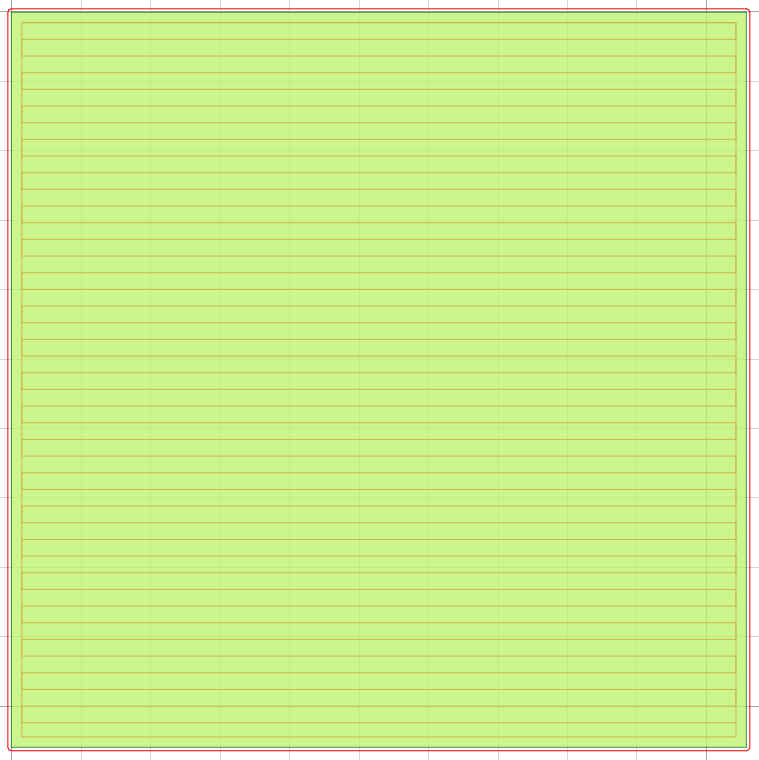
Result
Thanks
- FlatCAM practical tutorial: introduction, installation and import
- FlatCAM practical tutorial: copper traces geometry
- FlatCAM practical tutorial: clean non copper area
- FlatCAM practical tutorial: silkscreen geometry
- FlatCAM practical tutorial: contour
- FlatCAM practical tutorial: gcode and PCB milling
You can find Gerber, fritzing, images, and FlatCAM project files here.