
FlatCAM practical tutorial: copper traces geometry – Part 2
Now we have a base project to start work on. The first step is to create a series of geometries that become the passes used by CNC to isolate the copper traces.
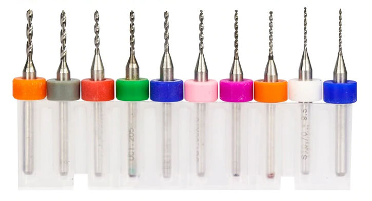
For all the milling working, I use these types of bits
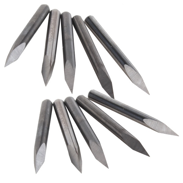
You can find here AliExpress
I prefer the 30° version because It’s more durable and works like a charm.
Now I must say that most of the operations result from experience, so you must know that these operations aren’t the better operations, but they are my better solution for milling PCB.
Generate trace isolation geometry
Now we are going to select with double click the Gerber PCB_PCF8574_03_copperBottom.gbl where we can find the information about the traces.
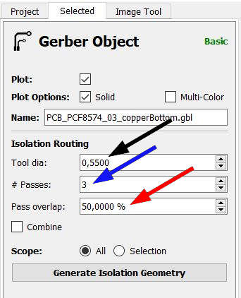
Now you have the Isolation routing panel, and here you have three-parameter:
- Tool dia (black): the diameter of the tool you are going to use
- # Passes (blue): the number of isolation passes you want (more passes more isolation of the trace)
- Pass overlap (red): the percentage of Tool dia to overlap between the pass
Now here I’d like to do a consideration, my idea is that we prefer possible copper area, because if there are some problem or auto level is not adequately set we don’t put out the work.
So I’d like to extend tool dia as much as possible. You check this parameter directly on the draw of the Geometry generated, search for the closest items, and check if the geometry is broken.
Here is an example with a tool size of 0.57
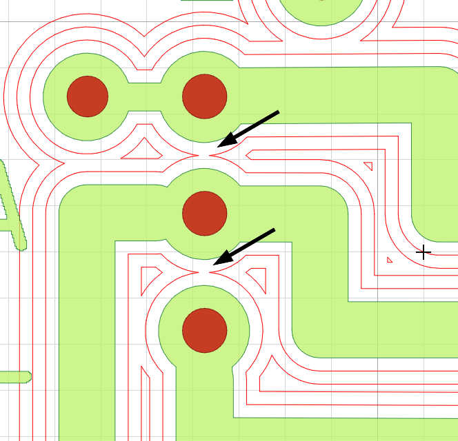
So I’m going to reduce the tool dia to 0.55, and the size permits the geometry to have the correct size.
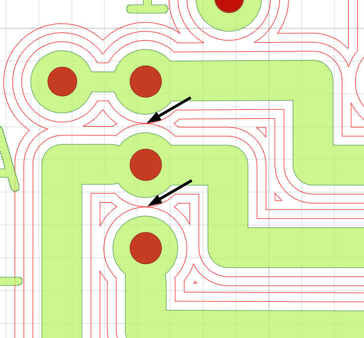
This is a perfect solution for me, the result is a clean board with a good quantity of copper, and you have a better result if you want more thin copper trace, but if you need more space from trace to trace (like for SMD), you must try more fitted Tool dia.
As you can see, I do three passes, and you can understand the mean of # Passes in the draw; this value is combined with Pass overlap that sets how much overlap, for example, with 50% overlap you have:
Or if you insert a 33% overlap
The idea is to remove as much copper as possible, so more extensive Pass overlap is better, but you must pay attention; first, we are using a bigger Tool dia, and 50% probably covers only 20% of the material.
If you use a too big overlap, the result is this
Here a correct pass overlap
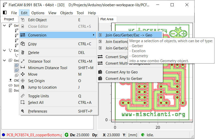
As you can see, there is a check Combine; this is quite useful if you check It instead to create one file for the pass.
PCB_PCF8574_03_copperBottom.gbl_iso1PCB_PCF8574_03_copperBottom.gbl_iso2PCB_PCF8574_03_copperBottom.gbl_iso3
It generates only one file with all three geometry
PCB_PCF8574_03_copperBottom.gbl_iso
I prefer to create 3 or 4 files and group only the first 2.
To group 2 or more geometry, you must select them with Shift + mouse click or Ctrl + mouse-click than going to Edit –> Conversion –> Join Geo/Gerber/Exc –> Geo; as a result, you obtain a new file with the join of the geometry you select.
I group only two geometry because I create a first gcode for this; I send the work to my CNC than If the isolation seems sufficient, I don’t do more; if It isn’t enough, I generate an additional gcode only for the third isolation geometry and so on with usually the limit of 5.
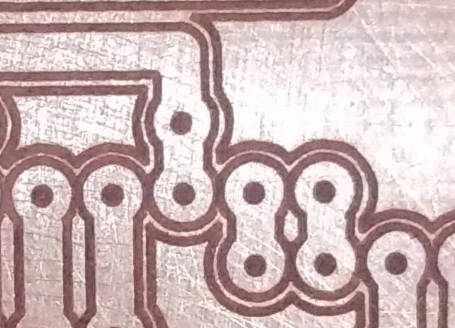
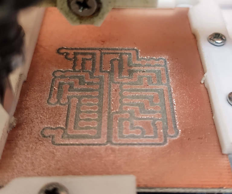
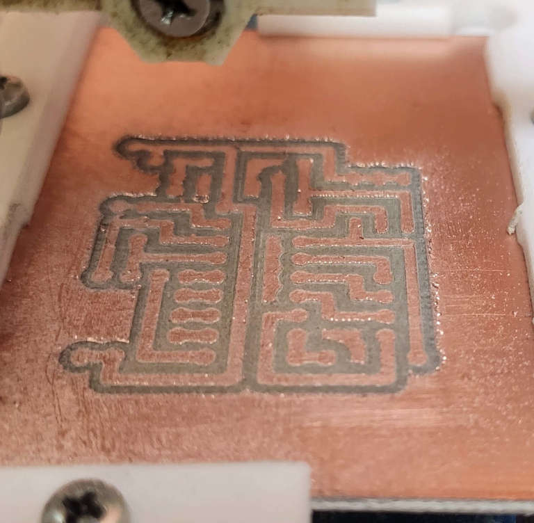
Here is an example of a single pass
beautiful but very difficult to solder and quite dangerous; humidity or dust can create a short circuit.
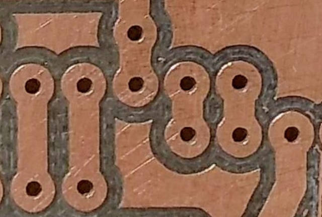
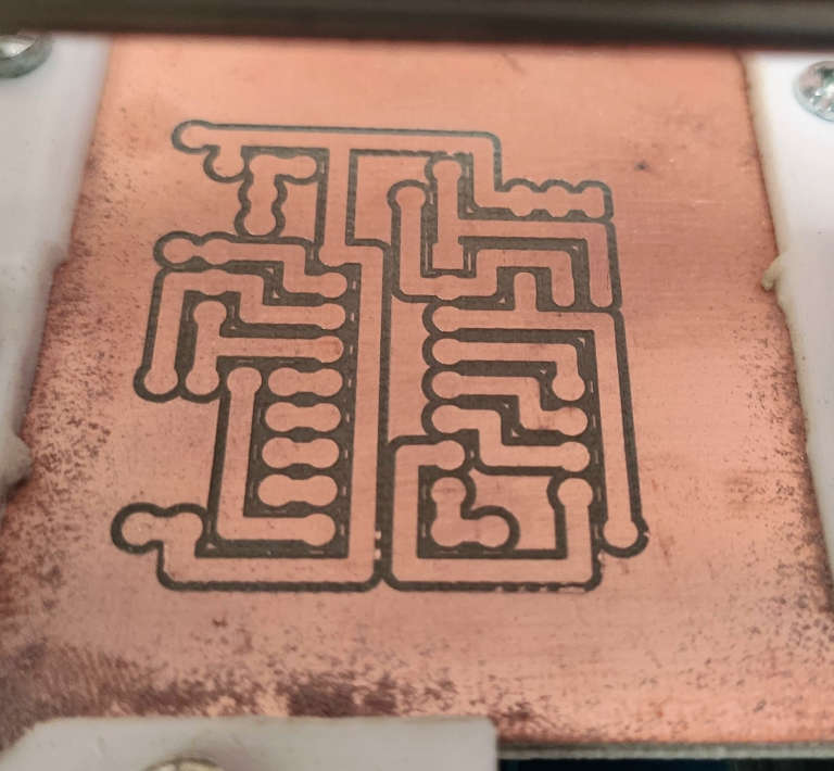
Result of first 2 passes
Don’t worry, the PCB isn’t clean, at the end when you clean It you get a good surprise.
The same but clean with sandpaper
Result last pass
Thanks
- FlatCAM practical tutorial: introduction, installation and import
- FlatCAM practical tutorial: copper traces geometry
- FlatCAM practical tutorial: clean non copper area
- FlatCAM practical tutorial: silkscreen geometry
- FlatCAM practical tutorial: contour
- FlatCAM practical tutorial: gcode and PCB milling
You can find Gerber, fritzing, images, and FlatCAM project files here.