Design and mill PCB: Easy and Cheap (Solder mask) – Part 5
Solder mask is used for protection against oxidation and to prevent solder bridges from forming between closely spaced solder pads. A solder bridge is an unintended electrical connection between two conductors by means of a small blob of solder. PCBs use solder masks to prevent this from happening. Another problem without solder mask is the possibility that an insect or dust can do a bridge between two conductors.
Material
You need some material, for the first time I use a very low cost tool:
UV curable solder mask resin
It’s a paint that dry when exposed to ultraviolet.
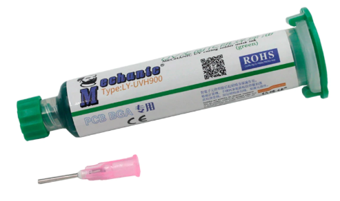
You can find here AliExpress
UV torch
It’s a torch with UV led, you can buy a low cost lamp.
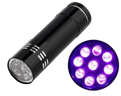
You can find here AliExpress
Full kit
Here the kit AliExpress
Torch holder
This type of torch is very poor so prepare you to expose for a long time the resin.
You can find project here.
Trasparent sheet
I used a trasparent sheet for my laser printer (Glorious Lexmark X642e), and put toner to max contrast.
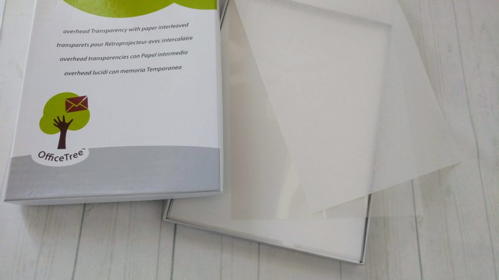
You can find here AliExpress
Credit card
I use a simple credit card to spread resin.
Rubber roller
To better spread resin It’s usefully a little rubber roller from 5 to 10cm.
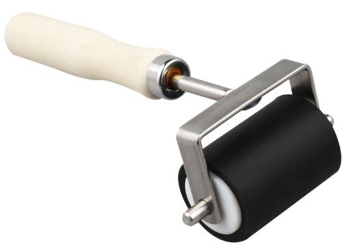
You can find here AliExpress
A glass
I put a glass over all to apply a pressure on sheet.
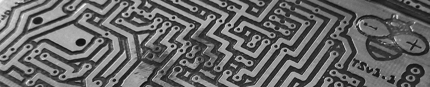
PCB
Naturally you need a PCB to apply resin 😉 .
Latex Gloves
Take gloves to prevent green on all surface.
Acetone
I use Acetone to clean residual of resin.
Process
When you have all the material you can start the process.
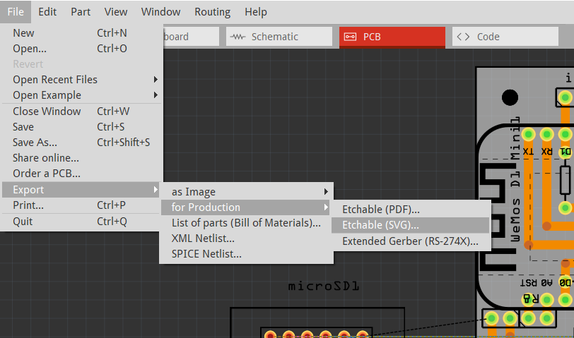
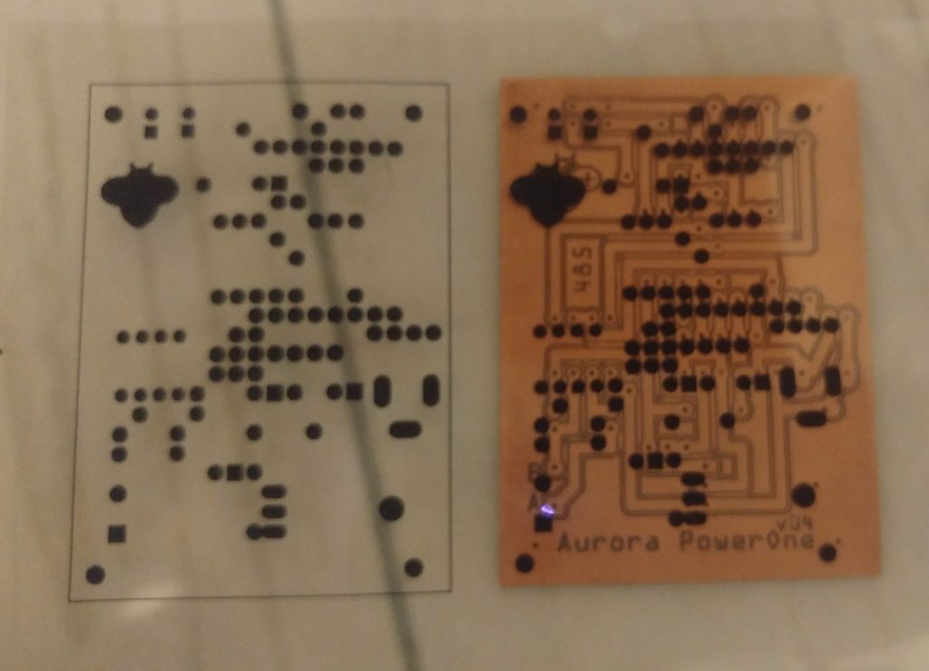
Generate svg file from fritzing
From Fritzing you can generate svg file for production (etching):
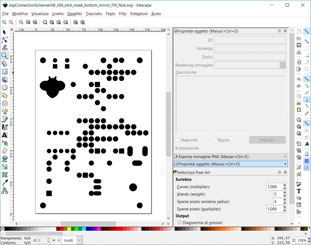
you need that file in particular you need a copper bottom mask. I’m going to fix something (logo) with Inkscape a beautiful and opensource vector graphics editor.
to print correctly I import svg file inside a LibreOffice draw
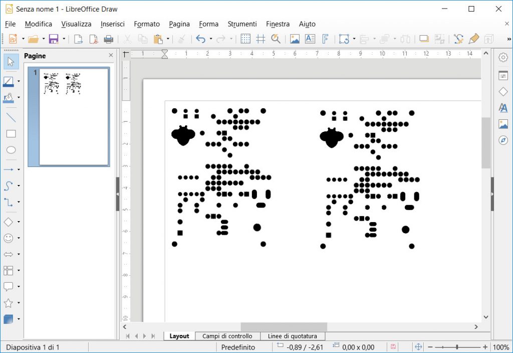
and the printed result
Printing:
- black white laser printer is better
- real size (no adapt to page size or similar)
- set toner at max intensity
- not set trasparent sheet select normal paper, if you set trasparent sheet the imprinting temperature is lower and print can be to low contrasted.
Prepare surface and clean the PCB
Take a surface where you can put all, remember resing can make It dirty. Than take Acetone and clean the PCB.
Put It over the surface.
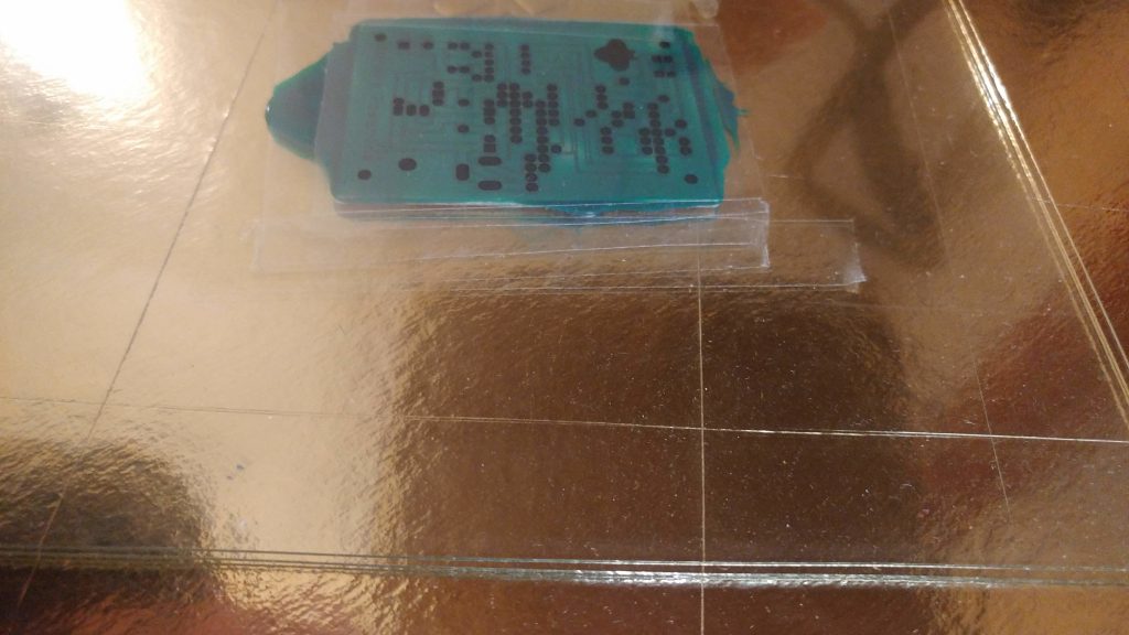
Use adhesive tape to apply, on one side only, a piece of transparent sheet to the surface.
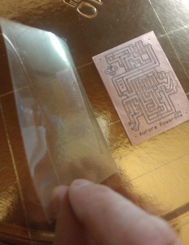
Apply resin
Put some resin over the PCB, than close attached transparent sheet over all and fix It on the other side.
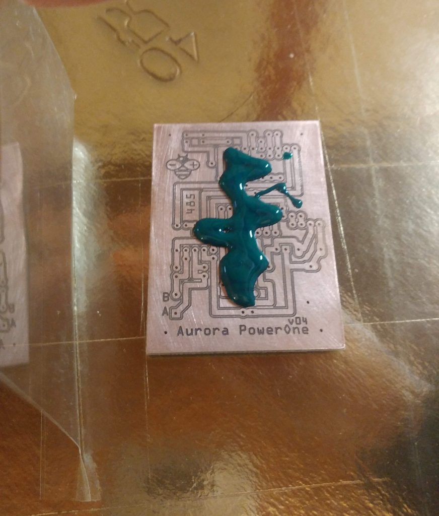
To prevent magin to thin It’s usefully to use a frame, I print one, but you can use a piece of PCB all around.
Use the credit card to spread evenly resin over all, remember the film must be thin.
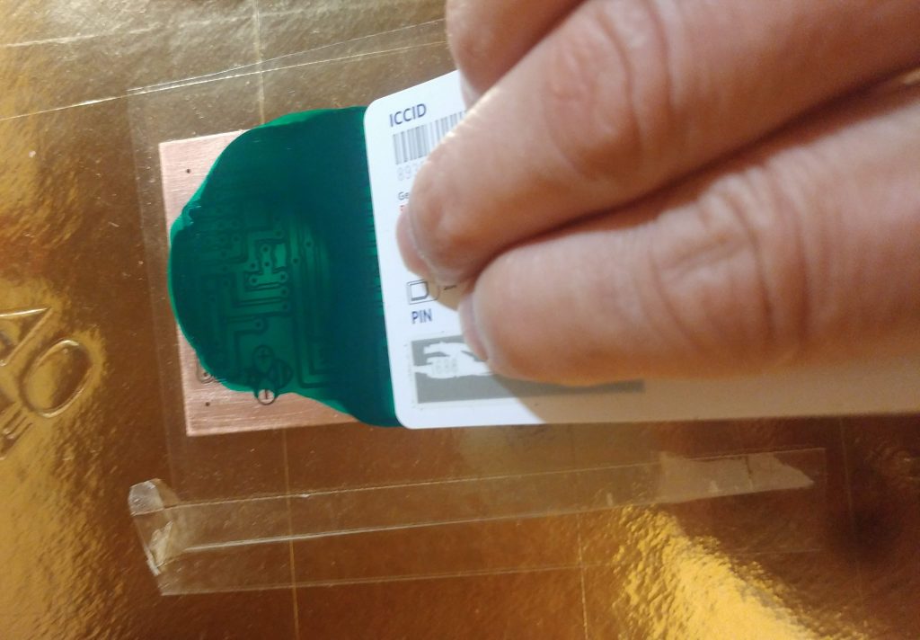
Now fix the other side with tape.
Somebody advise me to use a rubber roller to do It more thin and It’s true, rubber roller help to do this.
When all the resin is quite thin go ahead.
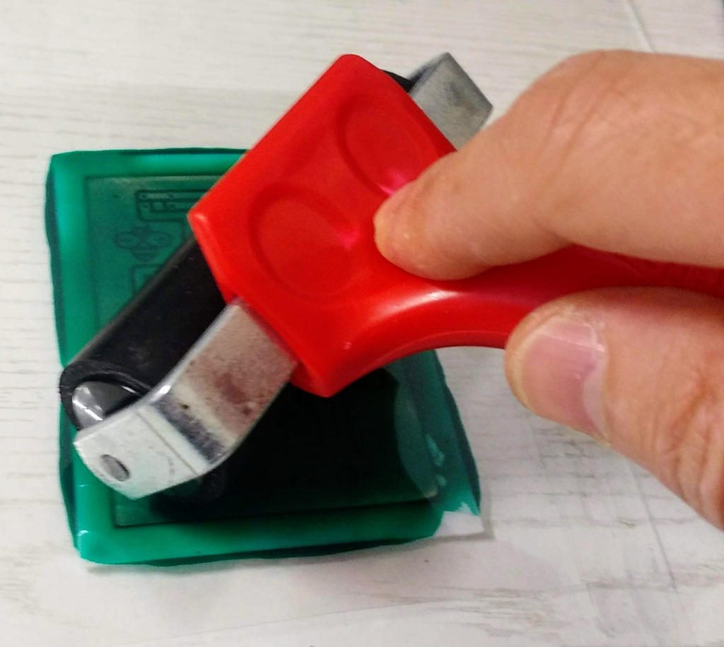
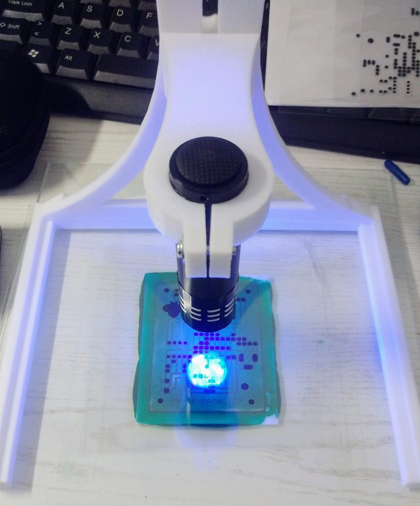
UV exposure
Take printed svg copper bottom mask and fix over the PCB, pay a lot of attention to the alignment of hole. Stop with tape.
I put over all a glass that help printed sheet to stay close.
Than take the lamp and light it on. With my poor torch the exposure time It’s about 40 minutes (with full battery less), if out there is the sun you can use It.
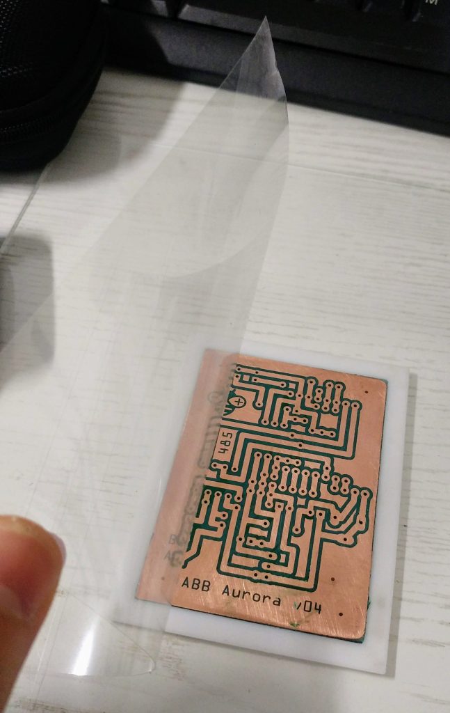
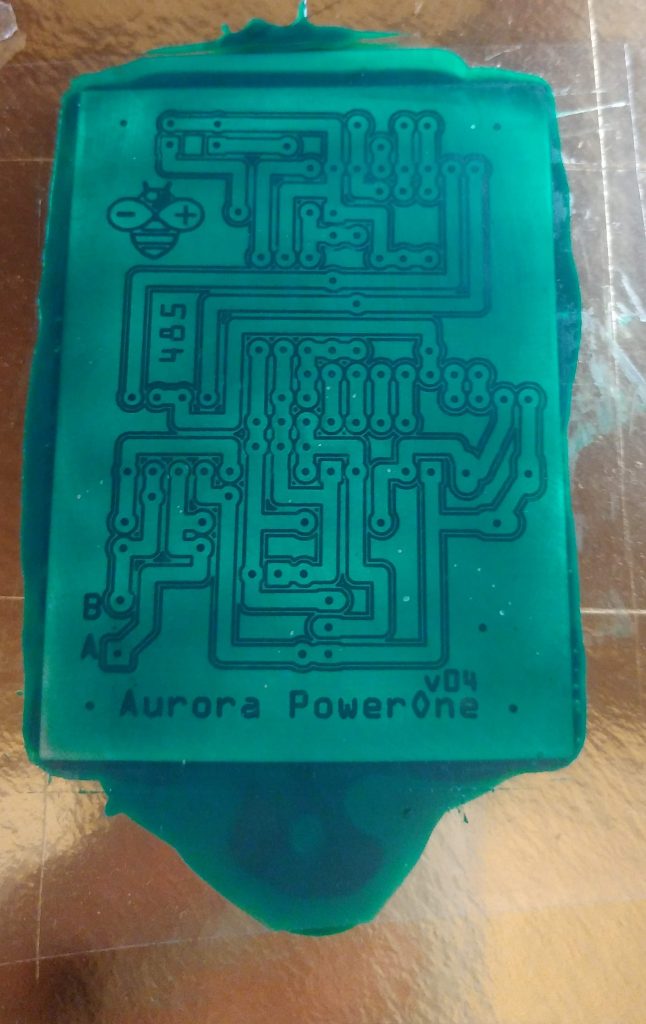
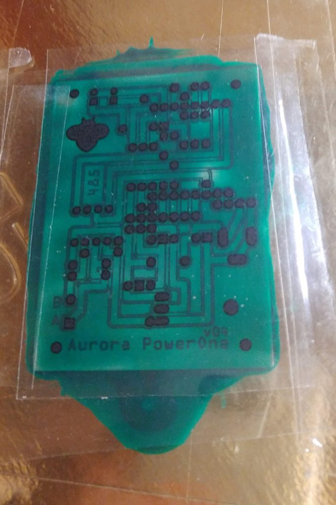
Remove waste
After some time you must remove the sheet, pay a lot of attention, curve the sheet and check if it detaches correctly from the sheet and not from the PCB.
Now take Acetone and remove the resin that not are exposed to UV.
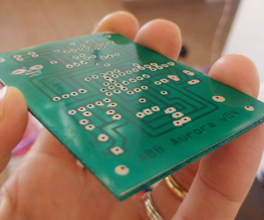
Take a needle and remove the resin from the hole.
After all put the PCB to the UV or sun to fix better the resin.


Hi Renzo, the Flatcam videos are very interesting.
I saw that on your website there is a tutorial where you make pcb with antisoldering mask but you use a UV lamp and a sheet with the pads painted black.
Can’t you do a tutorial where the paint on the pads are milled? I attach a link to show you better what I say.
Thanks a lot,
Hi Martin,
thanks for the suggestion, when I have some additional time I’m going to extend the flat cam tutorial.
Bye Renzo
Very nice. I like the idea of the roller. I will try to get one. Surrounding the pcb with 4 unprinted pcbs of similar size will reduce wasting the resin.
Thanks for the suggest Richard,
next time I’ll try It.
Bye Renzo